 | ÐлекÑÑоннÑй компоненÑ: HT81012 | СкаÑаÑÑ:  PDF PDF  ZIP ZIP |
Äîêóìåíòàöèÿ è îïèñàíèÿ www.docs.chipfind.ru
HT81XXX
EasyVoice
TM
Speech
Selection Table
Part No.
Mask
HT81003
HT81006
HT81009
HT81012
HT81018
OTP
HT81R03
HT81R09
HT81R18
HT81R36
Voice Capacity
3 sec
6 sec
9 sec
12 sec
18 sec
36 sec
Note:
The voice capacity is calculated based on 5kHz sampling rate.
For 3-second capacity HT81003/HT81R03 devices, refer to the its relevant data sheet.
Rev. 1.40
1
March 1, 2005
Features
·
Operating voltage: 2.4V~5V
·
Directly drives an external transistor
·
PWM function directly driver speaker
·
Low standby current (1
mA typ. for V
DD
=3V)
·
Minimal external components
·
240 notes table ROM for key functions
·
Programmable silence length and end-pulse width
(minimal end-pulse width is 1.3ms at 8kHz sampling
rate)
·
Controllable volume
·
FLAG1 options
-
End-pulse output
-
3Hz, 3HzB flash
-
6Hz, 6HzB flash
-
Busy output
-
OFF
·
FLAG2 options
-
3Hz flash
-
6Hz flash
-
Busy output
-
OFF
·
6 keys (Directed)
·
8 keys (Matrix key)
·
Key options
-
Sequential/Directed
-
Repeat (KEY2~KEY6)
-
STOP key (KEY6)
-
Key debounce time: 1.2ms, 22ms, 45ms
(based on a 8kHz sampling rate)
-
One shot/Normal
-
Pull-high resistance: 0, 50k
W, 100kW, 200kW
·
Section options
-
Retriggerable
-
Non-retriggerable
·
Dice form or 16-pin DIP package
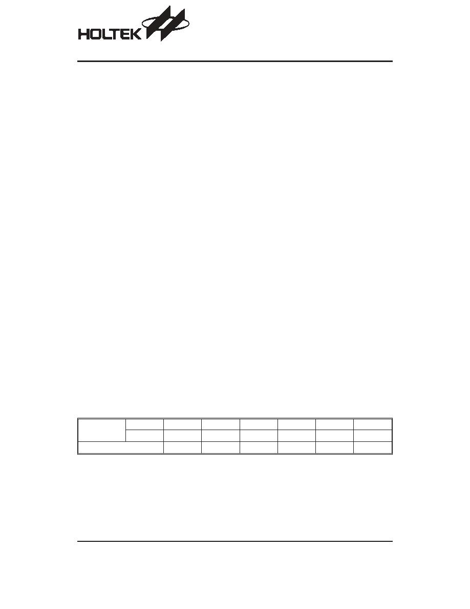
General Description
The EasyVoice
TM
is a single-chip voice synthesizer LSI .
The chip when triggered drives a speaker directly or
through an external transistor with a PWM output. Negli-
gible current is consumed in the standby state.
The HT81XXX provides direct key or Matrix key input
and 2 programmable FLAG outputs. With 2.4V~5.0V
power supply, a complete synthesized voice playback
system can be easily built with very few external compo-
nents.
The customer
¢s voice sources are recorded section by
section into an internal mask ROM. The instructions of
section playback arrangement of each key are stored in
the table ROM. The key features are also programma-
ble. With such a flexible structure, the EasyVoice
TM
is
excellent for versatile voice applications.
Applications
·
Leisure products
·
Alarm clocks
·
Alert and warning system
·
Sound effect generators
EasyVoice
TM
is a trademark of Holtek Semiconductor Inc.
Block Diagram
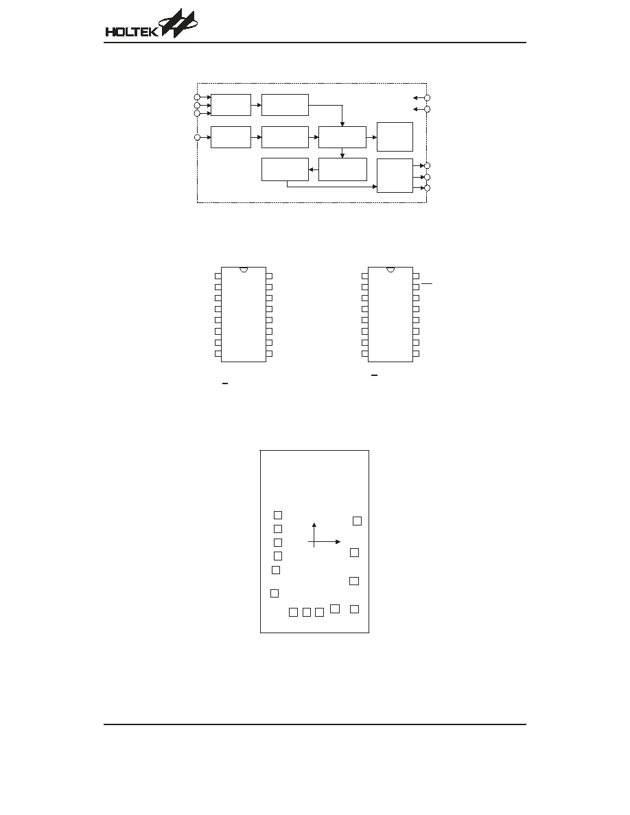
Pin Assignment
Pad Assignment
HT81006/HT81009
HT81XXX
Rev. 1.40
2
March 1, 2005
I / O 2
I / O 1
K E Y 4
V D D
O S C I
K E Y 1
K E Y 2
K E Y 3
V P P
V S S
O U T 3
V S S
O U T 2
V D D
O U T 1
1 6
1 5
1 4
1 3
1 2
1 1
1 0
9
1
2
3
4
5
6
7
8
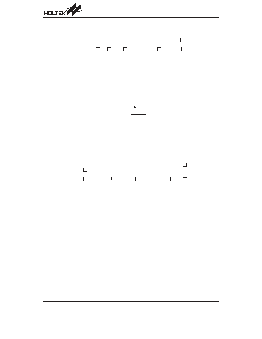
H T 8 1 R 0 9 / H T 8 1 R 1 8 / H T 8 1 R 3 6
1 6 D I P - A
O E
I / O 2
I / O 1
K E Y 4
V D D
O S C I
K E Y 1
K E Y 2
K E Y 3
N C
V S S
O U T 3
V S S
O U T 2
V D D
O U T 1
H T 8 1 0 0 6 / H T 8 1 0 0 9
H T 8 1 0 1 2 / H T 8 1 0 1 8
1 6 D I P - A
N C
1 6
1 5
1 4
1 3
1 2
1 1
1 0
9
1
2
3
4
5
6
7
8
D e b o u n c e
C i r c u i t
O n e - s h o t
O s c i l l a t o r
C i r c u i t
T i m e B a s e
G e n e r a t o r
R O M A d d r e s s
C o u n t e r
A u d i o
C o n t r o l l e r
D a t a R O M
I / O 1
I / O 2
S t a t u s
D i s p l a y
C o n t r o l l e r
V D D
V S S
O S C I
S e l e c t o r
O U T 2
O U T 3
O U T 1
K E Y 1 ~ 4
1
2
V D D
O S C I
K E Y 3
V S S
O U T 1
V D D
O U T 2
I / O 2
I / O 1
K E Y 4
K
E
Y
2
K
E
Y
1
O
U
T
3
V
S
S
3
4
5
6
7
8
9
1 0
1 1
1 2
1 3
1 4
( 0 , 0 )
Chip size: 41.9
´ 70.3 (mil)
2
* The IC substrate should be connected to VSS in the PCB layout artwork.
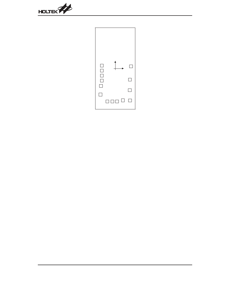
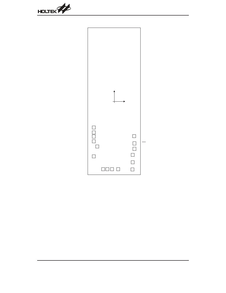
HT81012/HT81018
HT81XXX
Rev. 1.40
3
March 1, 2005
1
2
3
4
5
6
7
8
9
1 0
1 1
1 2
1 3
1 4
( 0 , 0 )
V D D
O S C I
K E Y 3
V S S
O U T 1
V D D
O U T 2
I / O 2
I / O 1
K E Y 4
K
E
Y
2
K
E
Y
1
O
U
T
3
V
S
S
Chip size: 41.9
´ 84.4 (mil)
2
* The IC substrate should be connected to VSS in the PCB layout artwork.
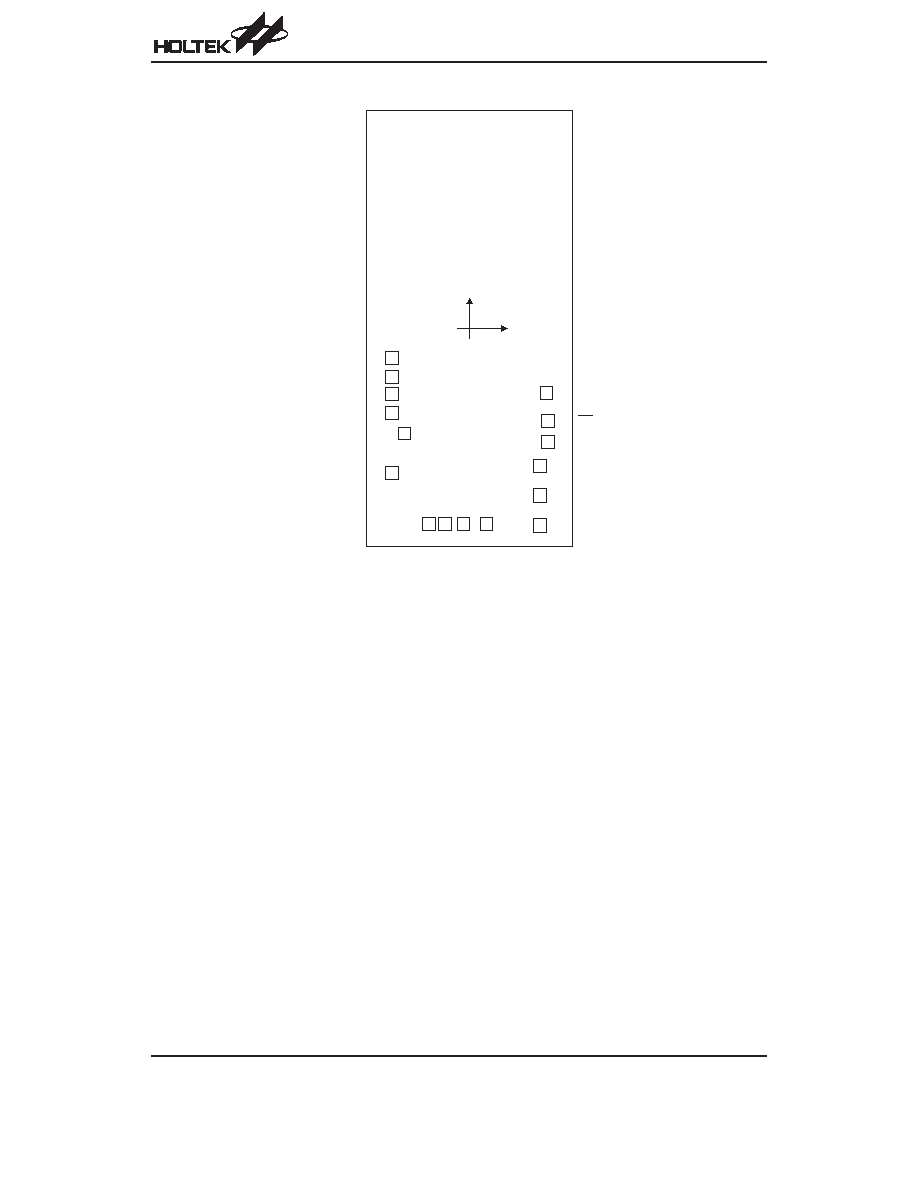
HT81R09
HT81XXX
Rev. 1.40
4
March 1, 2005
O S C I
K
E
Y
2
K
E
Y
1
O
U
T
3
V
S
S
O
U
T
2
9
1 0
1 1
V S S
O U T 1
V D D
K E Y 3
I / O 2
I / O 1
K E Y 4
V P P
O E
( 0 , 0 )
1 2
1 3
1
V D D
2
3
4
5
6
7
8
1 4
1 5
1 6
Chip size: 51
´ 102.8 (mil)
2
* The IC substrate should be connected to VSS in the PCB layout artwork.
HT81R18
HT81XXX
Rev. 1.40
5
March 1, 2005
1
2
3
4
5
6
7
8
9
1 0
1 6
1 5
1 4
1 3
1 2
1 1
( 0 , 0 )
V D D
O S C I
K E Y 3
V S S
O U T 1
V D D
I / O 2
I / O 1
K E Y 4
K
E
Y
2
K
E
Y
1
O
U
T
3
V
S
S
O
U
T
2
V P P
O E
Chip size: 51.6
´ 138 (mil)
2
* The IC substrate should be connected to VSS in the PCB layout artwork.
HT81R36
HT81XXX
Rev. 1.40
6
March 1, 2005
I
/
O
2
1
2
4
5
6
7
8
9
1 0
1 1
1 3
1 4
3
V
P
P
O
E
1 5
1 6
( 0 , 0 )
O
S
C
I
K
E
Y
2
K
E
Y
1
O
U
T
3
V
S
S
O
U
T
2
V S S
O U T 1
V D D
I
/
O
1
K E Y 3
K
E
Y
4
V D D
1 2
Chip size: 96.5
´ 121.1 (mil)
2
* The IC substrate should be connected to VSS in the PCB layout artwork.
Pad Coordinates
HT81006/HT81009
Unit:
mm
Pad No.
X
Y
Pad No.
X
Y
1
-342.450
254.150
8
-70.700
-672.700
2
-342.450
124.150
9
44.250
-672.700
3
-342.450
-7.700
10
191.500
-639.900
4
-342.450
-135.000
11
377.150
-646.800
5
-364.900
-272.350
12
373.200
-376.900
6
-376.670
-495.876
13
377.150
-107.000
7
-198.050
-672.700
14
401.150
200.700
HT81012/HT81018
Unit:
mm
Pad No.
X
Y
Pad No.
X
Y
1
-342.400
74.150
8
-70.700
-852.700
2
-342.400
-55.850
9
44.300
-852.700
3
-342.400
-187.700
10
191.550
-819.900
4
-342.400
-315.000
11
377.200
-826.800
5
-364.850
-452.350
12
373.250
-556.900
6
-376.620
-675.876
13
377.200
-287.000
7
-198.000
-852.700
14
401.200
20.700
HT81R09
Unit:
mm
Pad No.
X
Y
Pad No.
X
Y
1
-477.700
-173.500
9
-39.850
-1153.850
2
-477.700
-286.500
10
106.150
-1153.850
3
-477.700
-386.500
11
428.750
-1164.925
4
-477.700
-499.500
12
428.750
-988.600
5
-396.450
-621.950
13
428.750
-812.275
6
-476.100
-851.000
14
476.700
-669.700
7
-250.400
-1153.850
15
476.700
-547.424
8
-150.400
-1153.850
16
468.100
-377.600
HT81R18
Unit:
mm
Pad No.
X
Y
Pad No.
X
Y
1
-485.200
-621.000
9
-47.350
-1601.350
2
-485.200
-734.000
10
98.650
-1601.350
3
-485.200
-834.000
11
437.700
-1612.425
4
-485.200
-947.000
12
437.700
-1436.100
5
-403.950
-1069.450
13
437.700
-1259.775
6
-483.600
-1298.500
14
485.650
-1117.200
7
-257.900
-1601.350
15
485.650
-994.924
8
-157.900
-1601.350
16
477.050
-825.100
HT81XXX
Rev. 1.40
7
March 1, 2005
HT81R36
Unit:
mm
Pad No.
X
Y
Pad No.
X
Y
1
-800.500
1382.800
9
712.200
-1372.000
2
-1071.700
-1175.050
10
1053.500
-1372.000
3
-1066.600
-1372.000
11
1053.500
-1067.650
4
-468.200
-1361.000
12
1043.900
-874.750
5
-193.300
-1371.600
13
941.200
1389.700
6
43.900
-1371.600
14
513.175
1384.300
7
290.900
-1371.700
15
-210.400
1382.800
8
485.000
-1372.000
16
-555.200
1382.800
Pin Description
Pin No.
Pin Name
I/O
Internal Connection
Description
1
I/O2
I/O
NMOS Pull-high
Trigger key 6, active low/NMOS output
2
I/O1
I
NMOS Pull-high
Trigger key 5, active low/NMOS output
3
KEY4
I
Pull-high
Trigger key 4, active low
4
KEY3
I
Pull-high
Trigger key 3, active low
5, 12
VDD
¾
¾
Positive power supply
6
OSCI
I
Oscillator Input Pin
Oscillator input pin
7
KEY1
I
Pull-high
Trigger key 1, active low
8
KEY2
I
Pull-high
Trigger key 2, active low
9
OUT3
I/O
Pull-high Input/NMOS
Pull-high/transistor output/NMOS output
10, 14
VSS
¾
¾
Negative power supply, ground
11
OUT2
O
CMOS
PWM output
-/CMOS output
13
OUT1
O
CMOS
PWM output +/CMOS output
15, 16
NC
¾
¾
No connection - HT81R36 OTP device except
OE, VPP
¾
¾
HT81R36 OTP device only
Absolute Maximum Ratings
Supply Voltage ..........................V
SS
-0.3V to V
SS
+6.0V
Storage Temperature ..........................
-50°C to 125°C
Input Voltage ............................ V
SS
-0.3V to V
DD
+0.3V
Operating Temperature ..........................
-20°C to 70°C
Note: These are stress ratings only. Stresses exceeding the range specified under
²Absolute Maximum Ratings² may
cause substantial damage to the device. Functional operation of this device at other conditions beyond those
listed in the specification is not implied and prolonged exposure to extreme conditions may affect device reliabil-
ity.
HT81XXX
Rev. 1.40
8
March 1, 2005
Electrical Characteristics
Ta=25
°C
Symbol
Parameter
Test Conditions
Min.
Typ.
Max.
Unit
V
DD
Conditions
V
DD
Operating Voltage
3V
¾
2.4
3
5
V
I
DD
Operating Current
3V
No load
¾
1000
1200
mA
I
STB
Standby Current
3V
OSC stop
¾
1
3
mA
I
OL1
PWM Output Current
3V
V
OL
=0.2V
DD
90
110
¾
mA
I
OH1
3V
V
OH
=0.8V
DD
-10
-20
¾
I
OL2
I/O2 (TR)
3V
V
OL
=0.1V
DD
1
3
¾
mA
I
OH2
Tr Output Current
3V
V
OH
=0.9V
DD
-1
-2
¾
mA
I
OL3
I/O1 (FLAG Sink Current)
3V
V
OL
=0.1V
DD
3
5
¾
mA
V
IH
²H² Input Voltage
¾
¾
0.8V
DD
¾
V
DD
V
V
IL
²L² Input Voltage
¾
¾
0
¾
0.2V
DD
V
R
PH
Input Pull-high Resistor
3V
R=50k
W (option)
40
50
60
k
W
R=100k
W (option)
80
100
120
R=200k
W (option)
160
200
240
f
OSC
Oscillating Frequency
3V
R=110k
W (f
OSC
=2MHz)
1.6
2
2.4
MHz
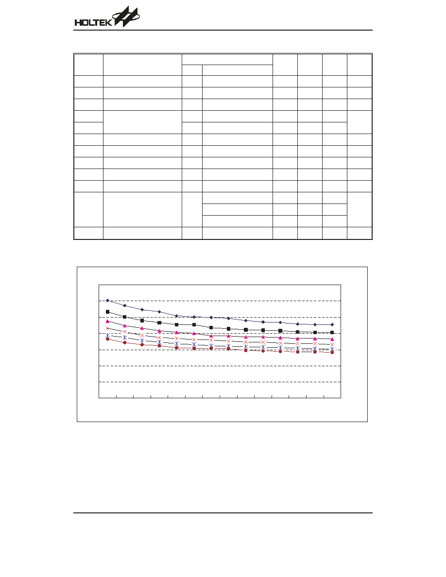
Characteristics Curve
HT81XXX
Rev. 1.40
9
March 1, 2005
2 . 4
2 . 6
2 . 8
3 . 0
3 . 2
3 . 4
3 . 6
3 . 8
4 . 0
4 . 2
4 . 4
4 . 6
4 . 8
5 . 0
V o l t a g e ( V )
3 . 5
3
2 . 5
2
1 . 5
1
0 . 5
0
R = 9 0 k W
R = 1 0 0 k W
R = 1 1 0 k W
R = 1 2 0 k W
R = 1 3 0 k W
R = 1 4 0 k W
F
r
e
q
u
e
n
c
y
(
M
H
z
)
V v s F C h a r a c t e r i s t i c s C u r v e
HT81XXX
Rev. 1.40
10
March 1, 2005
Functional Description
The EasyVoice
TM
is voice synthesizer with 6, 9, 12, 18 or
36-second voice capacity. A group of pre-recorded voice
sections is played upon receipt of key trigger input sig-
nals. Two FLAG signals are output while playing voices.
The HT81XXX voice capacity can be divided into sec-
tions of arbitrary length. Notice that the silence length
and end-pulse width are not included in the memory.
By using Holtek
¢s programming tools (HT-VDS81W),
the contents and arrangement of sections, as well as
key features and FLAG output are all programmable be-
fore device fabrication.
The IC provides 6 direct key inputs (KEY1~KEY6),
KEY1 can be optioned as a direct, sequential trigger
key. KEY2~KEY6 can be selected as a stop or a direct
key.
The IC provides matrix key (KEY1~KEY8), 6 program-
ming pins (KEY1, KEY2, KEY3, KEY4, I/O1 and I/O2)
can be divided to 8 key that can be optioned as normal
or one shot trigger.
Play Function Block Diagram
System Oscillator
The EasyVoice
TM
has a built-in RC oscillator which re-
quires only one external resistor for normal applications.
The oscillator frequency is typically 2MHz for an exter-
nal resistor of 150k
W. The required oscillator frequency
may vary with different sampling rates in the process of
voice programming. As a result, the value of the oscilla-
tor resistor may be different with respect to different
items.
The oscillator is turned on when triggered by a key input.
After playing, it is immediately turned off. Then the chip
goes into the standby state.
Voice ROM
The voice ROM is originally designed to continuously re-
cord the 6, 9, 12, 18 or 36-sec voice data at about 5kHz
sampling rate. A higher sampling rate will generate
voices of better playback quality, but will shorten the to-
tal recording time. On the other hand, a lower sampling
rate will result in longer recording time but sacrifice the
voice quality.
The playback time can be significantly extended by
making use of coding efficiency, silence playing, section
repeating, section cascade, etc.
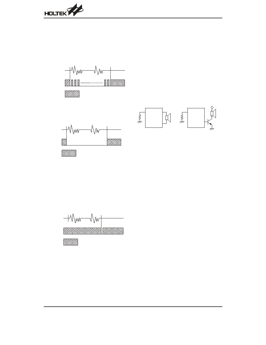
Section
Section is the basic element constituting the contents of
the voice ROM. During programming, the customer¢s
voice sources can be divided into as many sections as
required. A section can be composed of a voice or an in-
terval of silence. However, the silent length is not
counted in the voice ROM. The total number of sections
included should be less than 240 due to the space limi-
tation of the function table ROM. The total length of the
included sections is limited by the voice ROM.
A section, when triggered by a key input, can be played
once, repeatedly or cascaded with other sections, de-
pending on the key function table instructions.
The following are examples of section division:
In addition, a section can be set as retriggerable or
non-retriggerable depending on code option.
·
Retriggerable
When the currently playing section is set as
retriggerable, it will stop immediately upon receipt of
other key inputs.
·
Non-retriggerable
When the currently playing section is selected as
non-retriggerable, it will go on playing until the whole
section is completed, whether or not there is a key in-
put in the process of playing.
K e y
t r i g g e r
K e y
f e a t u r e s
o p t i o n
K e y
f u n c t i o n
t a b l e
R O M
V o i c e
R O M
S e l e c t
P l a y c o n t r o l l o g i c
F l a g
o u t p u t
V
D D
8 W
S P K
P W M +
P W M -
8 / 1 6 / 3 2 W
S P K
T R
H T 8 1 X X X
O S C I
R
O S C
s e c . 2
s e c . N
s e c . 1
s e c . 1
s e c . 2
s e c . 3
s e c . 1
R O M
E x a m p l e 1 : O n e s e c t i o n o n l y
E x a m p l e 2 : 3 s e c t i o n d i v i s i o n
E x a m p l e 3 : N s e c t i o n d i v i s i o n
R O M
R O M
HT81XXX
Rev. 1.40
11
March 1, 2005
For a key group, some sections can be set as
retriggerable and some as non-retriggerable. When a
retriggerable section of a key group is playing, any key
can be triggered to interrupt its playing. If it is a
non-retriggerable section playing, any key interrupt is
invalid.
Group
The EasyVoice
TM
plays groups according to the key in-
put. A group can be made up of one or more sections.
When a key is triggered, the corresponding group is
played. For example, triggering KEY2 plays group 2,
and so on. The same section is allowed to appear in dif-
ferent groups. However, KEY1 can be made up of multi-
ple groups when it is optioned as a sequential key.
Otherwise, each key is composed by one group only.
Key Function Table
The voice ROM sections are played according to the in-
structions of the key function table. The function table
contains group information and the playing order of the
sections in the groups. Notice that the total amount of
sections included in the groups should be less than 256
which is the space limitation of the function table ROM.
·
KEY1 as a direct key
Each key is mapped to a group in the function table. If
a key is not used, the group mapped to that key is a
piece of silence. The following is an example of the
function table:
Group 1
sec.1 + sec.2 + sec.3 + sec.4
Group 2
sec.3
As illustrated in the table, voice ROM is composed of 4
sections, and 5 sections for the function table. If KEY1
is momentarily triggered, section 1, section 2, section
3 and section 4 are played in sequence and then
stopped. Triggering KEY2 plays section 3.
·
KEY1 as a sequential key
When KEY1 is optioned as a sequential key, it can in-
clude multiple groups (sub-groups) in the function ta-
ble. However, KEY2 is used as a direct key exclusively
and comprise of only one group in the function table.
An example is shown below:
Group 1-1
sec.4 + sec.2
Group 1-2
sec.1 + sec.3
:
:
:
:
Group 1-N
sec.2 + sec.3
Group 2
sec.2 + sec.3
As indicated in the above table, KEY1 can be made up
of sub-groups. The corresponding sub-groups is
played in sequence each time KEY1 is triggered.
¨
The playing sequence of sequential KEY1 is:
Group 1-1
® Group 1-2 ® Group 1-3 ..... ® Group
1-N (the last group)
® Group 1-1 .....
¨
Reset of KEY1 playing sequence
If a sub-group of KEY1 group is being played and
KEY2 is triggered, the playing sub-group will be ter-
minated, and the newly triggered key group is played
in stead. The first sub-group will start playing by
retriggering KEY1. In other words, the KEY1 playing
sequence is reset whenever a key other than KEY1
is triggered (see Figure 1).
¨
Sub-group selection
When KEY1 is triggered with pulses, a desired
sub-group can be selected by controlling its corre-
sponding pulse number. However, the features of
KEY1 have to be set in the following ways:
-
Sequential
-
Retriggerable
-
Minimum key debounce time (
@1.2ms, f
OSC
=2MHz)
For instance, if sub-group 1-3 is the previous playing
group, sub-group 1-5 will start playing after 2 pulses
are applied to KEY1, and so on.
To make a selection of KEY1 sub-groups more easy,
KEY2 should be programmed as silence. Then this si-
lence key has to be triggered to reset KEY1. By so do-
ing, the playing sub-group of KEY1 is directly
specified by the pulse number applied to KEY1 (see
Figure 2).
G r o u p 1 - 1
G r o u p 1 - 2
G r o u p 1 - N
G r o u p ( 2 ~ 8 )
G r o u p 1 - 1
K E Y 1
K E Y 2
A U D
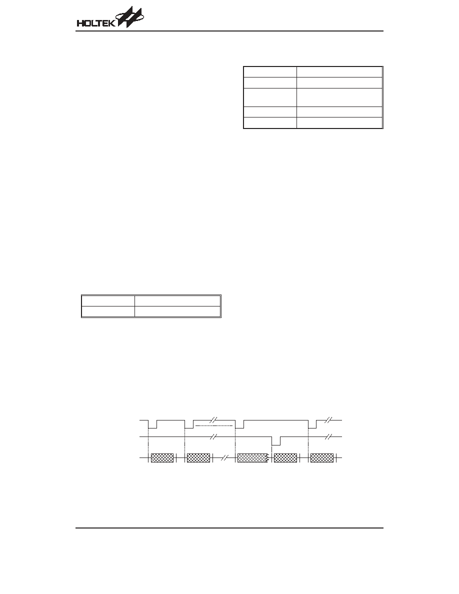
Figure 1. Reset of KEY1 Playing Sequence
HT81XXX
Rev. 1.40
12
March 1, 2005
·
KEY6 as a stop key (by mask option)
When KEY6 functions as a stop key, any voice output
can be stopped by pressing KEY6.
·
KEY2~KEY6 as a repeat key
As a repeat key, the sections included can be played
sequentially and repeatedly until other key input is
triggered.
Key Features
·
Key priority
When six keys are triggered simultaneously, the out-
put voice is determined by the key priority as shown
below:
KEY1>KEY2>KEY3>KEY4>KEY5>KEY6
·
Key debounce time
There are three kinds of key-in debounce time to be
selected by mask option, namely, 1.2ms, 22ms,
45ms. The key debounce time varies with the value of
the system frequency.
·
Pull-high resistance
Four kinds of key input pin pull-high resistance can
be selected by mask option, namely, 0k
W, 50kW,
100k
W and 200kW. The resistance may vary with
VDD, temperatures and the chip itself due to pro-
cess variations.
·
Trigger mode
The two keys can optioned as one-shot trigger mode
or normal mode.
¨
One shot
When one of the six keys (KEY1~ KEY6) is pressed
momentarily or held down, the group corresponding
to that key will play once.
¨
Normal trigger
When one of the two keys is pressed and held
down, the corresponding group will continue play-
ing. Once the pressed key is released, the group
will not stop until the included sections are all com-
pleted.
FLAG
When voices are playing, both FLAG1 and FLAG2 pins
are activated to output one of the following signals
through code option.
FLAG1 can be optioned as one of the following signal
outputs:
OFF, 3HzB flash, Busy, 6HzB flash, 3hz, 6Hz or End-pulse
output
FLAG2, on the other hand, can be set as one of the fol-
lowing signal outputs:
OFF, 3Hz flash, 6Hz flash, or Busy output.
·
3Hz/3HzB flash
When voices are playing, FLAG1 as well as FLAG2
pin outputs a 3Hz signal to drive a LED. The signal is
active low, 25% duty. Once the voice output is termi-
nated, the FLAG1 and FLAG2 pins become floating
outputs. When the FLAG1 and the FLAG2 pins are
optioned as 3HzB and 3Hz output, they will alternately
output at a 3Hz rate.
G r o u p N
G r o u p N
K E Y N
A U D
G r o u p 1 - N
N p u l s e
G r o u p 1 - M
M p u l s e
K E Y 1
K E Y 2
( S i l e n c e )
A U D
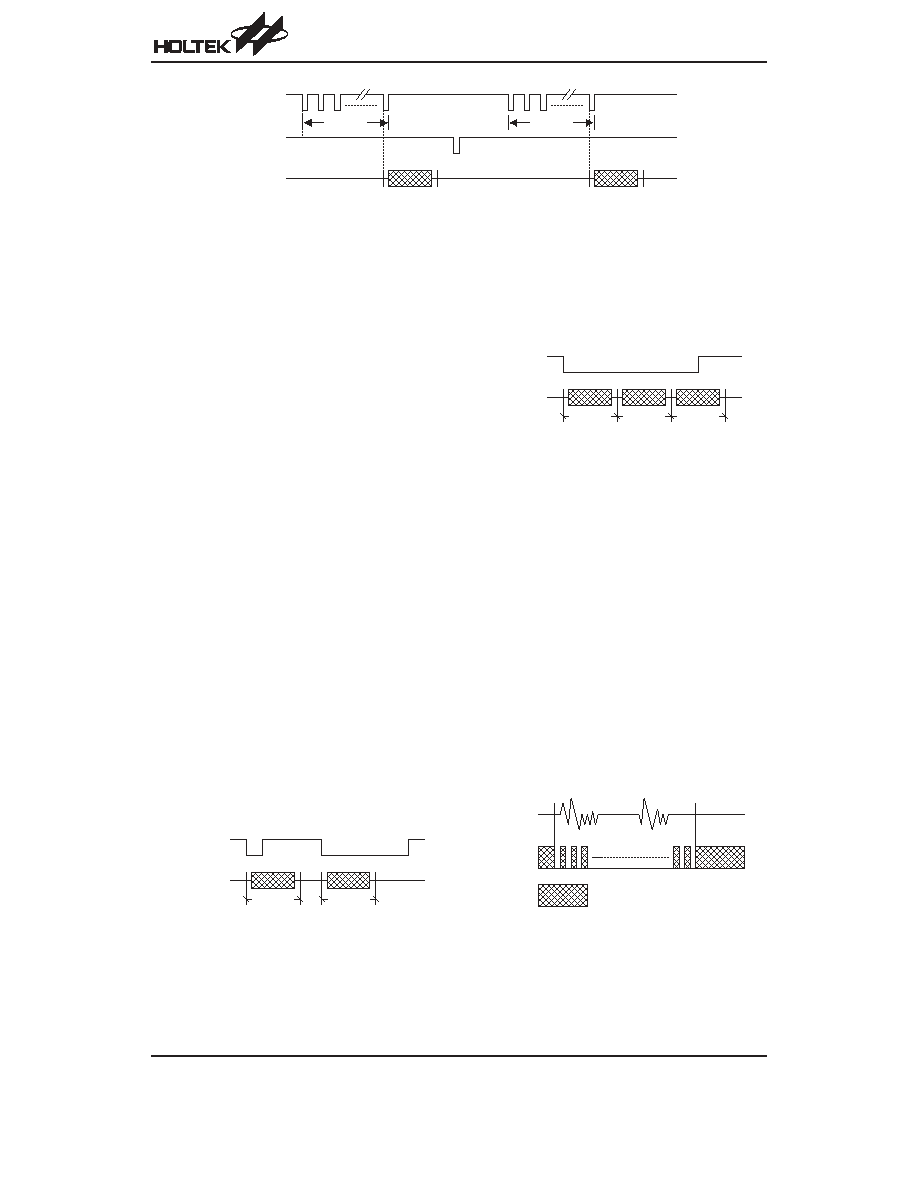
Figure 2. KEY1 Sub-Group Selection
G r o u p N
G r o u p N
G r o u p N
K E Y N
A U D
A U D
F L A G
: F l o a t i n g
HT81XXX
Rev. 1.40
13
March 1, 2005
·
6Hz/6HzB flash
When voices are playing, the FLAG1 pin outputs a
6Hz signal to drive a LED. The signal is active low,
25% duty. Once the voice output is terminated, the
FLAG1 pin becomes a floating output. When the
FLAG1 and the FLAG2 pins are optioned as 6HzB
and 6Hz outputs, they will alternately output at a
6Hz rate.
·
Busy output
When a voice group is playing, the outputs of both
FLAG1 and FLAG2 are turned low, indicating that the
chip is busy.
In addition to the above-stated output signals, FLAG1
can also generate one of the following signals by code
option:
¨
End-pulse output
When the voice output is completed, the FLAG1 pin
outputs an active low pulse. The pulse width can be
programmed depending on the customer
¢s require-
ments.
The FLAG1 as well as FLAG2 pins are both floating
outputs when the chip is in the standby state.
Volume Control
The function of the volume control can be set by mask
option. A code is written in the function table for the pur-
pose of controlling the volume of each section output af-
ter the volume control function is chosen. There are two
volume options, namely; full range and half range.
I/O2
The I/O2 pin is a PWM structure. It outputs voice signals
to drive a speaker through an external NPN transistor
when the chip is active. The OUT1 and OUT2 pins are
configured as PWM structure which can drive 8/16/32
W
speaker directly.
An 8050 type transistor with h
FE
@150 is recommended
for an output driver.
A U D
F L A G
: F l o a t i n g
A U D
F L A G
: F l o a t i n g
O U T 1
O S C I
O U T 2
R
O S C
H T 8 1 X X X
S P K
O U T 3
S P K
V
D D
O S C I
R
O S C
H T 8 1 X X X
A U D
F L A G
: F l o a t i n g
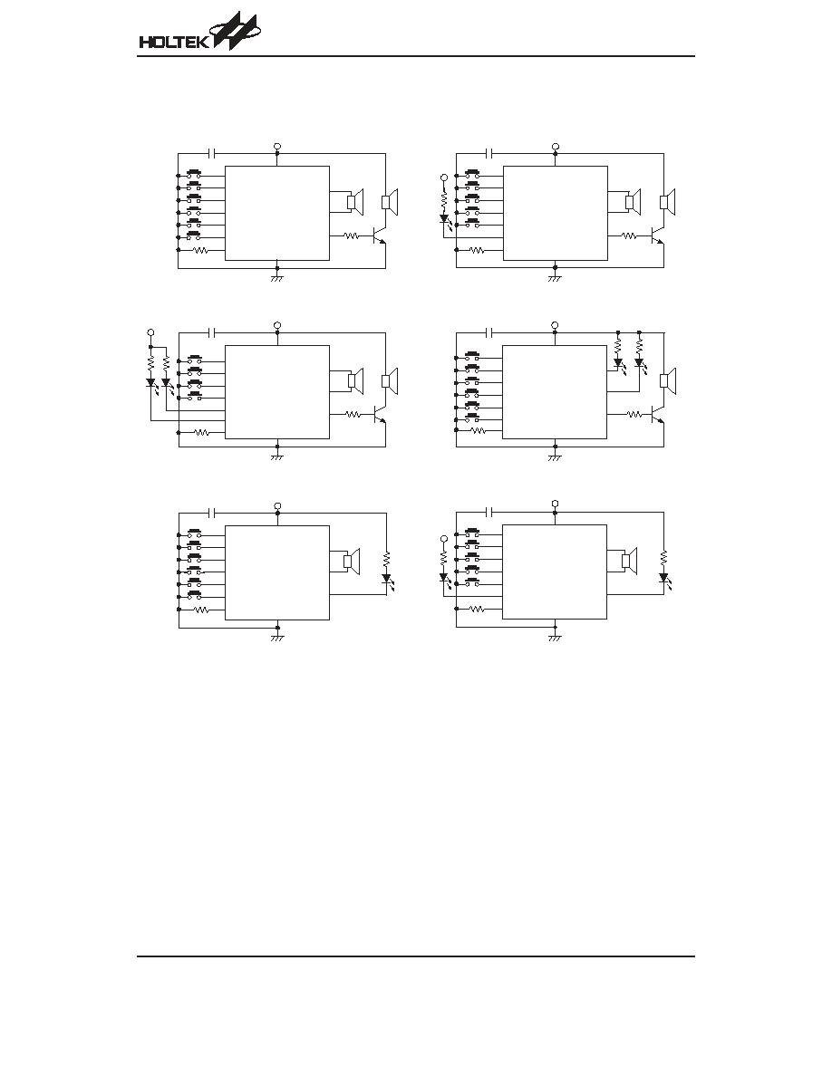
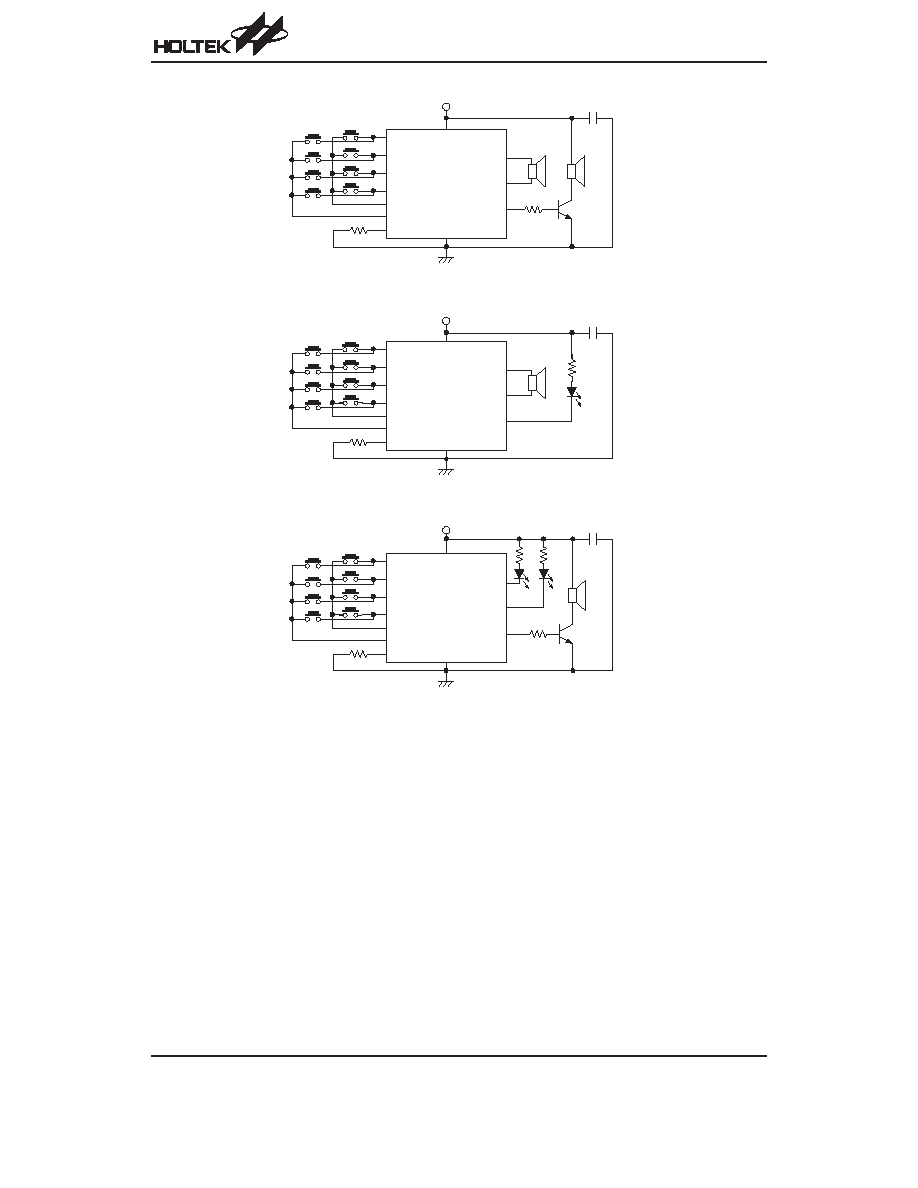
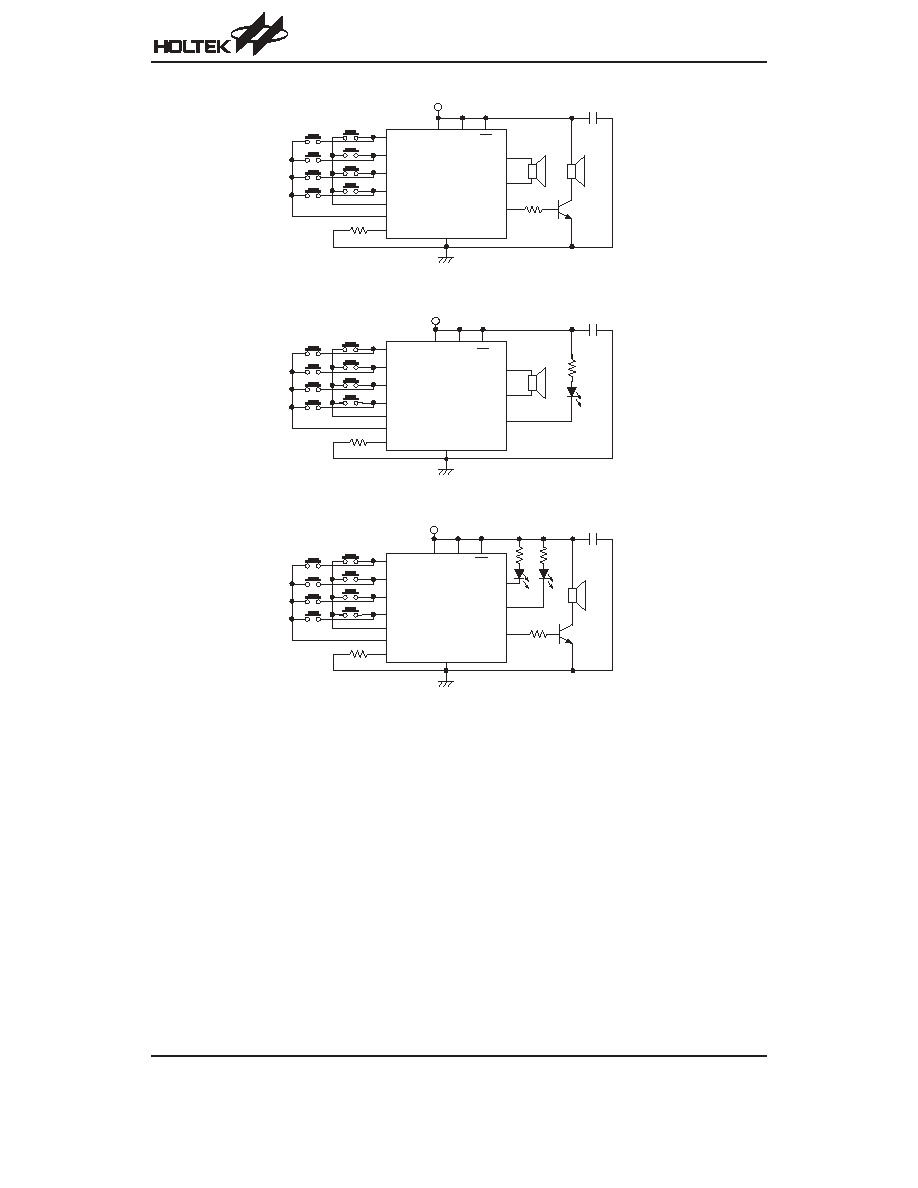
Application Circuits
Mask Type
HT81XXX
Rev. 1.40
14
March 1, 2005
H T 8 1 X X X
O S C I
R
O S C
V D D
V S S
O U T 1
O U T 2
O U T 3
V
D D
0 . 1 m F
8 W
S P K
H T 8 1 X X X
V S S
0 . 1 m F
8 0 5 0
H T 8 1 X X X
V S S
O U T 1
O U T 2
O U T 3
0 . 1 m F
2 0 0 W
H T 8 1 X X X
V S S
0 . 1 m F
K E Y 1
K E Y 2
K E Y 2
K E Y 1
K E Y 3
K E Y 4
K E Y 4
K E Y 3
I / O 1
I / O 2
K E Y 6
K E Y 5
O U T 1
O U T 2
O U T 3
2 0 0 W
5
1
0
W
8 0 5 0
5
1
0
W
O U T 1
O U T 2
O U T 3
8 / 1 6 / 3 2 W
S P K
8 W
S P K
8 0 5 0
K E Y 1
K E Y 2
K E Y 2
K E Y 1
K E Y 3
K E Y 4
K E Y 4
K E Y 3
I / O 1
I / O 2
K E Y 5
O S C I
R
O S C
K E Y 1
K E Y 2
K E Y 2
K E Y 1
K E Y 3
K E Y 4
K E Y 4
K E Y 3
I / O 1
I / O 2
K E Y 5
K E Y 1
K E Y 2
K E Y 2
K E Y 1
K E Y 3
K E Y 4
K E Y 4
K E Y 3
I / O 1
I / O 2
5
1
0
W
5
1
0
W
8 0 5 0
K E Y 6
O S C I
R
O S C
8 / 1 6 / 3 2 W
S P K
8 W
S P K
8 / 1 6 / 3 2 W
S P K
8 W
S P K
H T 8 1 X X X
O S C I
R
O S C
V S S
O U T 1
O U T 2
O U T 3
0 . 1 m F
8 / 1 6 / 3 2 W
S P K
H T 8 1 X X X
V S S
0 . 1 m F
K E Y 1
K E Y 2
K E Y 2
K E Y 1
K E Y 3
K E Y 4
K E Y 4
K E Y 3
I / O 1
I / O 2
K E Y 6
K E Y 5
O U T 1
O U T 2
O U T 3
8 / 1 6 / 3 2 W
S P K
K E Y 1
K E Y 2
K E Y 2
K E Y 1
K E Y 3
K E Y 4
K E Y 4
K E Y 3
I / O 1
I / O 2
K E Y 5
O S C I
R
O S C
5
1
0
W
5
1
0
W
V D D
V
D D
V D D
V
D D
V D D
V
D D
V D D
V
D D
V D D
V
D D
V
D D
R
O S C
O S C I
V
D D
5
1
0
W
5
1
0
W
V
D D
2 0 0 W
HT81XXX
Rev. 1.40
15
March 1, 2005
H T 8 1 X X X
V S S
O U T 1
O U T 2
O U T 3
K E Y 1
K E Y 2
K E Y 2
K E Y 1
K E Y 3
K E Y 4
K E Y 4
K E Y 3
I / O 1
I / O 2
K E Y 6
K E Y 5
K E Y 8
K E Y 7
O S C I
R
O S C
0 . 1 m F
H T 8 1 X X X
V S S
O U T 1
O U T 2
O U T 3
K E Y 1
K E Y 2
K E Y 2
K E Y 1
K E Y 3
K E Y 4
K E Y 4
K E Y 3
I / O 1
I / O 2
K E Y 6
K E Y 5
K E Y 8
K E Y 7
O S C I
R
O S C
0 . 1 m F
8 / 1 6 / 3 2 W
S P K
H T 8 1 X X X
V S S
O U T 1
O U T 2
O U T 3
2 0 0 W
K E Y 1
K E Y 2
K E Y 2
K E Y 1
K E Y 3
K E Y 4
K E Y 4
K E Y 3
I / O 1
I / O 2
8 0 5 0
K E Y 6
K E Y 5
K E Y 8
K E Y 7
O S C I
R
O S C
0 . 1 m F
8 / 1 6 / 3 2 W
S P K
8 W
S P K
5 1 0 W
2 0 0 W
5
1
0
W
8 0 5 0
5
1
0
W
8 W
S P K
V D D
V
D D
V D D
V
D D
V D D
V
D D
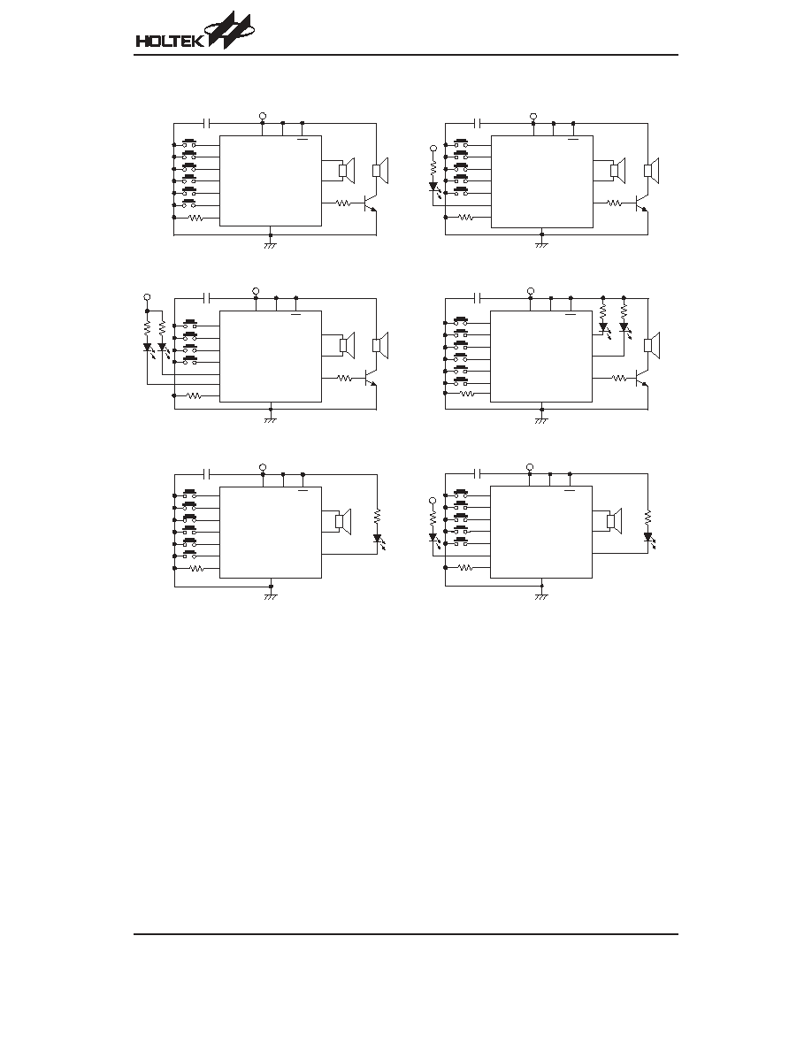
OTP Type
HT81XXX
Rev. 1.40
16
March 1, 2005
H T 8 1 R X X
O S C I
R
O S C
V D D
V S S
O U T 1
O U T 2
O U T 3
V
D D
0 . 1 m F
8 W
S P K
H T 8 1 R X X
V S S
0 . 1 m F
8 0 5 0
H T 8 1 R X X
V S S
O U T 1
O U T 2
O U T 3
0 . 1 m F
2 0 0 W
H T 8 1 R X X
V S S
0 . 1 m F
K E Y 1
K E Y 2
K E Y 2
K E Y 1
K E Y 3
K E Y 4
K E Y 4
K E Y 3
I / O 1
I / O 2
K E Y 6
K E Y 5
O U T 1
O U T 2
O U T 3
2 0 0 W
5
1
0
W
8 0 5 0
5
1
0
W
O U T 1
O U T 2
O U T 3
8 / 1 6 / 3 2 W
S P K
8 W
S P K
8 0 5 0
K E Y 1
K E Y 2
K E Y 2
K E Y 1
K E Y 3
K E Y 4
K E Y 4
K E Y 3
I / O 1
I / O 2
K E Y 5
O S C I
R
O S C
K E Y 1
K E Y 2
K E Y 2
K E Y 1
K E Y 3
K E Y 4
K E Y 4
K E Y 3
I / O 1
I / O 2
K E Y 5
K E Y 1
K E Y 2
K E Y 2
K E Y 1
K E Y 3
K E Y 4
K E Y 4
K E Y 3
I / O 1
I / O 2
5
1
0
W
5
1
0
W
8 0 5 0
K E Y 6
O S C I
R
O S C
8 / 1 6 / 3 2 W
S P K
8 W
S P K
8 / 1 6 / 3 2 W
S P K
8 W
S P K
H T 8 1 R X X
O S C I
R
O S C
V S S
O U T 1
O U T 2
O U T 3
0 . 1 m F
8 / 1 6 / 3 2 W
S P K
H T 8 1 R X X
V S S
0 . 1 m F
K E Y 1
K E Y 2
K E Y 2
K E Y 1
K E Y 3
K E Y 4
K E Y 4
K E Y 3
I / O 1
I / O 2
K E Y 6
K E Y 5
O U T 1
O U T 2
O U T 3
8 / 1 6 / 3 2 W
S P K
K E Y 1
K E Y 2
K E Y 2
K E Y 1
K E Y 3
K E Y 4
K E Y 4
K E Y 3
I / O 1
I / O 2
K E Y 5
O S C I
R
O S C
5
1
0
W
5
1
0
W
V P P
O E
V D D
V
D D
V P P
O E
V D D
V
D D
V P P
O E
V D D
V
D D
V P P
O E
V D D
V
D D
V P P
O E
V D D
V
D D
V P P
O E
V
D D
V
D D
V
D D
O S C I
R
O S C
5
1
0
W
2 0 0 W
5
1
0
W
HT81XXX
Rev. 1.40
17
March 1, 2005
H T 8 1 R X X
V S S
O U T 1
O U T 2
O U T 3
K E Y 1
K E Y 2
K E Y 2
K E Y 1
K E Y 3
K E Y 4
K E Y 4
K E Y 3
I / O 1
I / O 2
K E Y 6
K E Y 5
K E Y 8
K E Y 7
O S C I
R
O S C
0 . 1 m F
H T 8 1 R X X
V S S
O U T 1
O U T 2
O U T 3
K E Y 1
K E Y 2
K E Y 2
K E Y 1
K E Y 3
K E Y 4
K E Y 4
K E Y 3
I / O 1
I / O 2
K E Y 6
K E Y 5
K E Y 8
K E Y 7
O S C I
R
O S C
0 . 1 m F
8 / 1 6 / 3 2 W
S P K
H T 8 1 R X X
V S S
O U T 1
O U T 2
O U T 3
2 0 0 W
K E Y 1
K E Y 2
K E Y 2
K E Y 1
K E Y 3
K E Y 4
K E Y 4
K E Y 3
I / O 1
I / O 2
8 0 5 0
K E Y 6
K E Y 5
K E Y 8
K E Y 7
O S C I
R
O S C
0 . 1 m F
8 / 1 6 / 3 2 W
S P K
8 W
S P K
5 1 0 W
2 0 0 W
5
1
0
W
8 0 5 0
5
1
0
W
8 W
S P K
V D D
V
D D
V P P
O E
V D D
V
D D
V P P
O E
V D D
V
D D
V P P
O E
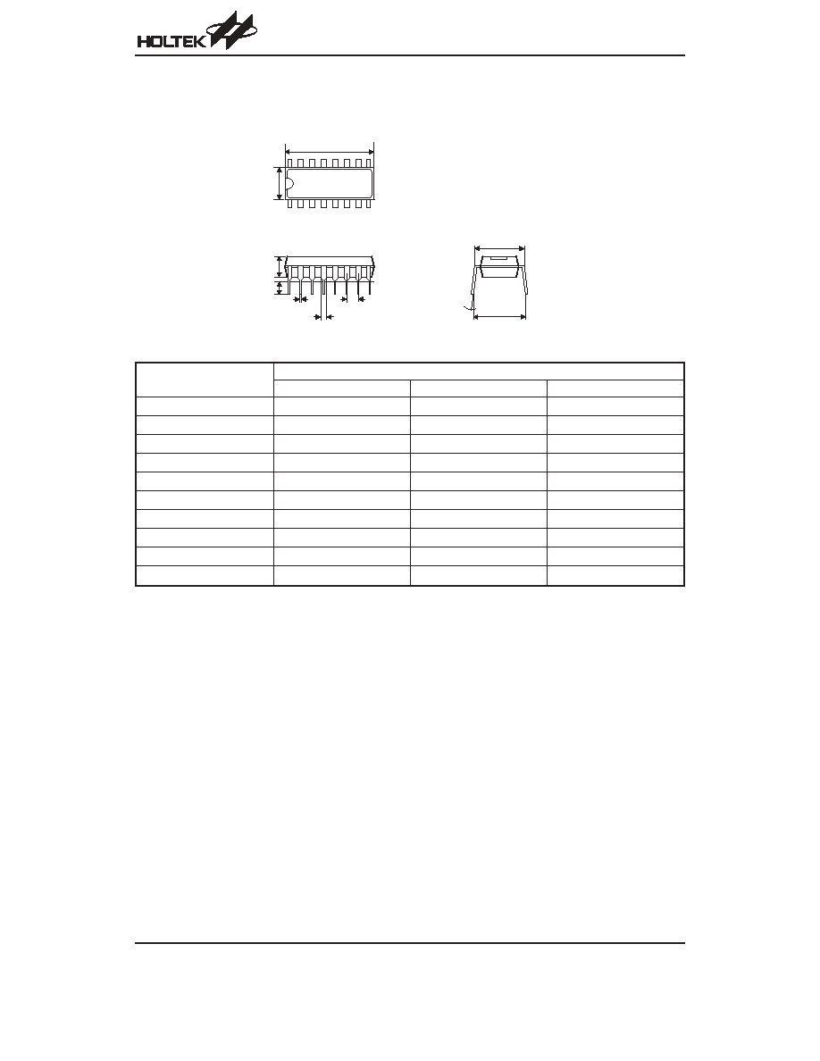
Package Information
16-pin DIP (300mil) Outline Dimensions (Plastic)
Symbol
Dimensions in mil
Min.
Nom.
Max.
A
745
¾
775
B
240
¾
260
C
125
¾
135
D
125
¾
145
E
16
¾
20
F
50
¾
70
G
¾
100
¾
H
295
¾
315
I
335
¾
375
a
0
°
¾
15
°
HT81XXX
Rev. 1.40
18
March 1, 2005
a
1 6
1
9
8
A
B
C
D
E
F
G
H
I

HT81XXX
Rev. 1.40
19
March 1, 2005
Holtek Semiconductor Inc. (Headquarters)
No.3, Creation Rd. II, Science Park, Hsinchu, Taiwan
Tel: 886-3-563-1999
Fax: 886-3-563-1189
http://www.holtek.com.tw
Holtek Semiconductor Inc. (Taipei Sales Office)
4F-2, No. 3-2, YuanQu St., Nankang Software Park, Taipei 115, Taiwan
Tel: 886-2-2655-7070
Fax: 886-2-2655-7373
Fax: 886-2-2655-7383 (International sales hotline)
Holtek Semiconductor Inc. (Shanghai Sales Office)
7th Floor, Building 2, No.889, Yi Shan Rd., Shanghai, China 200233
Tel: 021-6485-5560
Fax: 021-6485-0313
http://www.holtek.com.cn
Holtek Semiconductor Inc. (Shenzhen Sales Office)
43F, SEG Plaza, Shen Nan Zhong Road, Shenzhen, China 518031
Tel: 0755-8346-5589
Fax: 0755-8346-5590
ISDN: 0755-8346-5591
Holtek Semiconductor Inc. (Beijing Sales Office)
Suite 1721, Jinyu Tower, A129 West Xuan Wu Men Street, Xicheng District, Beijing, China 100031
Tel: 010-6641-0030, 6641-7751, 6641-7752
Fax: 010-6641-0125
Holmate Semiconductor, Inc. (North America Sales Office)
46712 Fremont Blvd., Fremont, CA 94538
Tel: 510-252-9880
Fax: 510-252-9885
http://www.holmate.com
Copyright
Ó 2005 by HOLTEK SEMICONDUCTOR INC.
The information appearing in this Data Sheet is believed to be accurate at the time of publication. However, Holtek as-
sumes no responsibility arising from the use of the specifications described. The applications mentioned herein are used
solely for the purpose of illustration and Holtek makes no warranty or representation that such applications will be suitable
without further modification, nor recommends the use of its products for application that may present a risk to human life
due to malfunction or otherwise. Holtek
¢s products are not authorized for use as critical components in life support devices
or systems. Holtek reserves the right to alter its products without prior notification. For the most up-to-date information,
please visit our web site at http://www.holtek.com.tw.
Document Outline
- þÿ
- þÿ
- þÿ
- þÿ
- þÿ
- þÿ
- þÿ
- þÿ
- þÿ
- þÿ
- þÿ
- þÿ
- þÿ
- þÿ
- þÿ